A team at Monash University has built a tiny chip that does something no integrated device has done before: it can generate, steer and read out information carried by light all in one place — at room temperature, on a footprint the size of a fingernail.
The work, published in Nature Photonics and announced in early June, addresses a long-standing roadblock in a field called valleytronics, where information is encoded in a quantum property of electrons known as the "valley degree of freedom." Researchers have spent years showing that valleytronics could enable faster, cooler and more efficient computing — but they could only do one piece of the job at a time. Building a full system on a single chip had remained out of reach.
Until now.
One Chip, Three Jobs
"Until now, we could generate or detect these signals, but not do everything in one integrated device," said lead author Dr. Chi Li of the Monash School of Physics and Astronomy. "What we've built is a complete on-chip system that can create, route and read this information with very high precision."
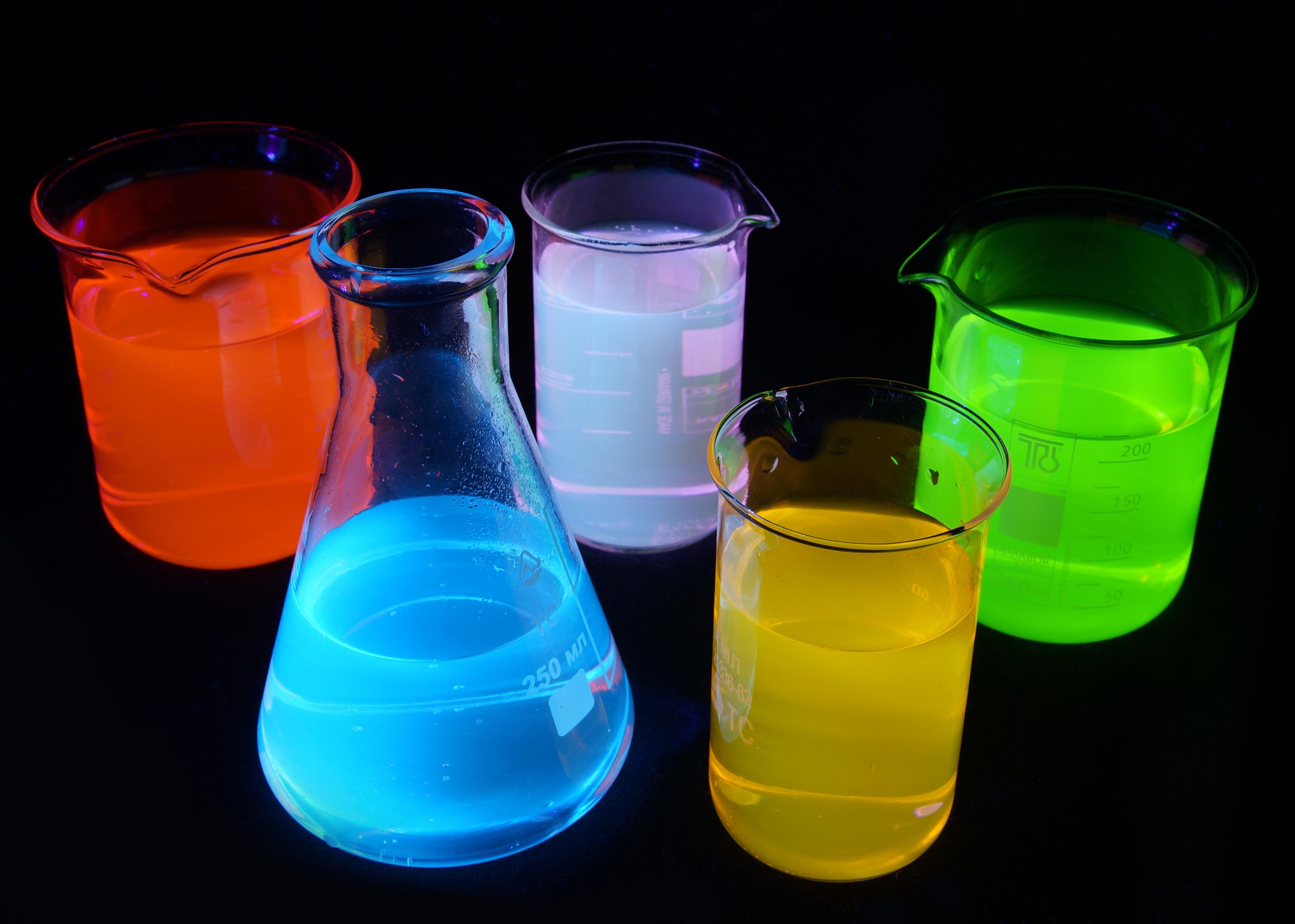
The device pairs ultra-thin materials only a few atoms thick with specially engineered metasurfaces — patterned nanostructures designed to control light at scales smaller than the wavelength of the light itself. Co-first author Dr. Kaijian Xing said the team used a straightforward "stacking" approach to combine the two-dimensional materials with the metasurfaces, sidestepping the very tricky process of growing one directly on top of the other.
The result is a single device that can:
- Generate specialized "valley" light signals
- Steer them along defined optical paths on the chip
- Convert them into electrical signals at the readout end
Why "Room Temperature" Matters
Many quantum systems only work when cooled to within a hair of absolute zero, which requires bulky cryogenic equipment and large amounts of power. The Monash chip works at room temperature, which dramatically lowers the cost and complexity of deploying it in the real world.
"This is a significant step toward scalable, chip-based technologies that use light instead of electricity to process information," said senior author Dr. Haoran Ren, an ARC Future Fellow who leads Monash's NanoMeta Group. "Photonic devices use light to achieve massive bandwidths, ultra-fast data transmission speeds, and lower energy consumption."
That combination — bandwidth, speed and efficiency — is exactly what is needed to keep up with the rising demands of AI workloads, secure communications and next-generation imaging. Conventional electronic chips are running into thermal and power limits as transistors continue to shrink. Photonics offers a way past those limits by replacing many of the moving electrons with photons.
A Practical Step in a Long Race
Valleytronics has been studied since researchers began exfoliating two-dimensional materials such as graphene and transition-metal dichalcogenides in the 2000s. The promise has always been more information per photon — a kind of extra "label" that can be carried alongside polarization and phase. But the gap between a lab demonstration and a deployable chip has remained wide.
The Monash integration closes part of that gap. By combining generation, routing and detection on a single device, the team has built a foundation that other groups can build on. The next steps will involve scaling the device, programming it for specific tasks, and testing it inside larger photonic systems used for quantum computing, optical neural networks and secure data links.
The takeaway for the broader photonic-computing race is straightforward: integration matters as much as raw performance. Discrete light sources, modulators and detectors are well understood, but each interface between them costs energy and adds noise. Putting them on one chip is what makes the technology practical — and that is the step Monash has just shown is possible.